Ghidra Loader for Super Mario Bros. 3 NES ROM
in Super Mario Bros. 3 Ghidra Loader / Ghidra-plugin

I’ve completed a Ghidra loader that correctly maps in all the ROM’s program banks at their respective addresses along with all of the symbols from the complete disassembly located on GitHub.
This loader currently does not allow analysis flow into or out of banks that are swapped in/out during runtime (all banks but two), as described in the post below.
For those unfamiliar with the Super Mario Bros. 3 speedrunning community, I have been doing reverse engineering and understanding the mechanics behind much of Super Mario Bros. 3 for the past year in order to find glitches or exploit logic in the game so as to support the top tier runners and their attempts to lower the world record times.
I helped develop the Early Hammer Manipulation and had a part in developing many of the new tech features in MitchFlowerPower’s ROM hack, Mini Kaizo Bros. 3.
TL;DR, Just Give Me the Code
The Super Mario Bros. 3 NES ROM Ghidra Loader source can be found on my GitHub at https://github.com/fortenbt/Ghidra-SMB3INES-Loader
Super Mario Bros. 3 NES ROM Versions
There were two versions of the Super Mario Bros. 3 US region cartridge: Rev 0 and Rev 1. Their respective ROM files are suffixed (U) (PRG0) [!] and (U) (PRG1) [!]. The only major visual difference between the two are the names of the Worlds as shown during the end credits after beating the game. The different names are shown in the table below.
| US (Revision 0) | US (Revision 1) |
|---|---|
| Grass Land | Grass Land |
| Desert Hill | Desert Land |
| Ocean Side | Water Land |
| Big Island | Giant Land |
| The Sky | Sky Land |
| Iced Land | Ice Land |
| Pipe Maze | Pipe Land |
| Castle of Koopa | Dark Land |
Other than that, there’s some minor differences in the location of some routines in bank 31.
Captain Southbird’s disassembly assembles byte-for-byte into the PRG1 version of the ROM, and therefore the symbols and their addresses in the loader are matched to that ROM.
MMC3 Mapper and Banking
The total size of the Super Mario Bros. 3 NES ROM is 393,232 bytes. There is a 16-byte INES header followed by the actual cartridge contents. The cartridge contents are broken up into the PRG ROM (program memory) consisting of 32 banks of 8,192-byte blocks of 6502 code and the CHR ROM (character memory) consisting of 128 blocks of 1,024-byte graphics data.
However, the 6502 processor only supports 16-bit addressing and was only designed to address 32 KB of PRG ROM in the 32 KB of address space from 0x8000 through 0xFFFF. RAM and other peripherals are mapped at lower memory addresses. In order to fit the entire game’s code in 32 KB, the MMC3 mapper hardware was used within the cartridge. This extra hardware allowed the process of banking to occur, where running code could write to special registers on the cartridge to swap in and out specific banks of the PRG code when it needed them. The NES memory map is shown in the following figure.
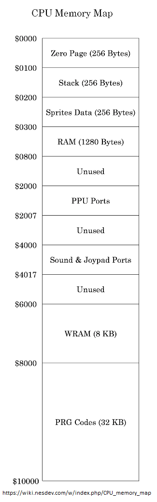 The NES CPU’s Memory Map
In Super Mario Bros. 3, banks 30 and 31 are always present at addresses 0x8000-0x9FFF and 0xE000-0xFFFF, respectively. All the other banks are written to exist at either 0xA000-0xBFFF or 0xC000-0xDFFF. This can easily be seen in Southbird’s complete disassembly in the main smb3.asm file, which uses the .include and .org macros to include the PRG bank files assembled at specific base addresses.
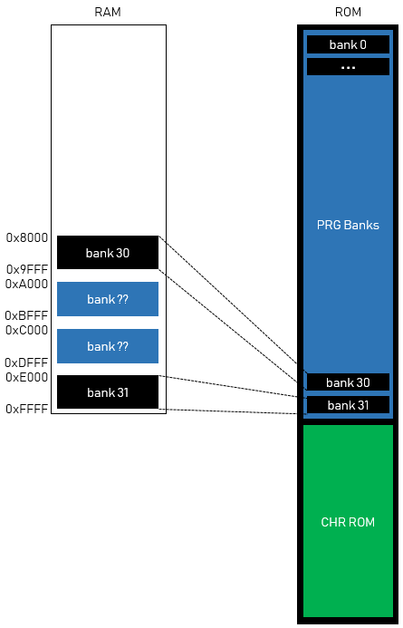 Only banks 30 and 31 are permanently mapped into RAM
Ghidra Memory Blocks
When beginning to write the Ghidra Loader, I was completely new to their API and really had no idea how I was meant to go about loading in each bank. I referenced multiple open source loaders for different formats to begin to find my way around. A few of these are listed below:
One of the things I noticed was that none of the open source projects I found really did anything similar to loading multiple code blocks at the same virtual address, something that was required for the MMC3 banking construct. Turning to Ghidra’s documentation, I found that it was really lacking for someone coming into the API completely new and looking to find an overview of the model or examples of how one might do different things.
After clicking through much of their object model, trying to keep it all straight in my head (it’s still confusing that you seem to be able to do the same thing from multiple different places within the object hierarchy), and after playing around with the memory space window in the GUI, it seemed like the best option would be to create a MemoryBlock for each bank, each one backed by the corresponding file contents of that bank.
I immediately got an error during loading saying that I had overlapping memory blocks:
Failed to add language defined memory block due to conflict: STACK @ 0x0100, length=0x1ff
Wait a minute, though…that’s a language-defined memory block called STACK at address 0x0100. I didn’t attempt to define that with my loader. Grepping through their source, I found some memory blocks defined in a file within a language directory called 6502.pspec. This processor spec file defined multiple blocks of memory by default for any 6502 binary loaded into Ghidra. This was broken by default!
The default memory blocks defined were:
  <default_memory_blocks>
    <memory_block name="IO" start_address="0" length="0x20" initialized="false"/>
    <memory_block name="LOW_RAM" start_address="0x20" length="0xff" initialized="false"/>
    <memory_block name="STACK" start_address="0x0100" length="0x01ff" initialized="false"/>
  </default_memory_blocks>
There was an “IO” block from 0x0 through 0x20, “LOW_RAM” from 0x20 through…0x1DF? That had to be wrong. In the 6502 architecture, addresses 0x0 through 0xFF are called the “zero page”, because those addresses can be accessed with a single byte (the high address byte is zero). This would make sense to define a default memory block from 0x0 through 0xFF called LOW_RAM, but this block started at 0x20 and its length was 0xFF. Even if the starting address was 0x0, the length of 0xFF would set the memory block to addresses 0x0 through 0xFE. Something was obviously overlooked.
I guessed that there used to be a “LOW_RAM” block defined from 0x0 through 0xFF, and that the pspec format used to specify start_address and end_address. At some point, there was a system with a 6502 processor that someone at the NSA was reverse engineering that had IO at addresses 0x0 through 0x20, so they modified the pspec file to support this.
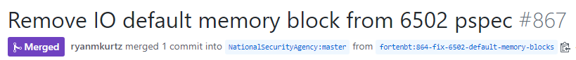
Eventually, the pspec file format was reworked and modified to take a length parameter, and loading a 6502 file never really got any attention. I went ahead and created an Issue and Pull Request in the Ghidra codebase, and it was recently merged.
 The fixed default memory blocks will be in Ghidra version 9.1
Overlay Memory Blocks and Virtual Addresses
After getting the default memory blocks to load without errors, the memory blocks I created were erroring out for the same reason. You apparently could not have multiple memory blocks defined that overlapped each other at the same virtual address. After looking over the API a bit more, I found that the MemoryBlock creation method took a Boolean argument called overlay. I wasn’t sure what this was, and there was no documentation describing it, but it sounded like exactly what I wanted.
Sure enough, when the memory blocks were overlay MemoryBlocks, multiple of them could be placed at a single virtual address without error.
Overlay Memory Block Limitations
The only way to load multiple binaries in at the same virtual address (as far as I could tell), was to use overlay MemoryBlocks. After placing each bank in a new overlay memory block and disassembling, I realized that if code within an overlay block accessed memory outside of that block, even if that memory was not in an overlay block, the disassembly code flow would not follow. It did appear that data symbols were resolved successfully, though.
Therefore, any calls to or from the banks that are swapped out are still not resolved. I don’t know of a way to fix this currently. To maximize the amount of logic flow, I created non-overlay memory blocks for banks 30 and 31, since those are never swapped out.
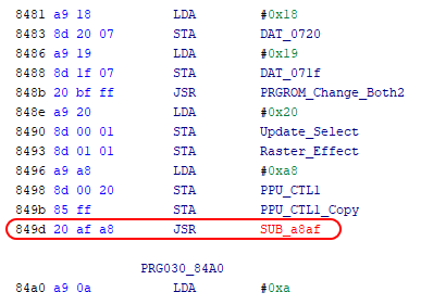 A call into a swappable bank or overlay memory block is not resolved
Symbols
Because of the huge amount of work Captain Southbird put into the disassembly, there are symbols for almost every function, data, and RAM variable in the game. The only file that contains all these symbols and their addresses, however, is one created during assembly of the game, called smb3.fns. This file contains a complete listing of every symbol and its address, in the following form:
; smb3.asm
Music_Sq2NoteOn                  = $E53D
PRG030_8E24                      = $8E24
Video_3CMAppear2                 = $830D
Inventory_DoPowerupUse           = $A40E
PRG024_BCD4                      = $BCD4
TAndK_DrawDiagBox                = $A0A7
Card_CursorYs                    = $D6E1
HostToad_SpriteYs_End            = $C714
UnusedBRL                        = $A930
; 11,500+ more lines...
; ...
As you can see, only symbols and addresses are present. This didn’t really help me, because I needed to know which bank those symbols were from in order to apply the symbol to the correct overlay memory block.
I wrote a Python script that parses each source assembly file for symbols and keeps track of which bank they were in. It then cross-references the list of symbols with the smb3.fns file to find the virtual address of the symbol in order to apply both the bank and the address to create the label in Ghidra. The Python script actually creates 32 .java files, one for each bank, that can be included directly in the Loader code.
NOTE: Please don’t judge the terrible Python script performance. I do realize I’m calling re.search in probably some O(n^2) way, but I knew it was correct and just wanted my symbols :P.
A Generic INES ROM Loader
I started this project with the goal of creating a generic INES ROM loader. I hadn’t really thought it all the way through, but I guessed that it would probably be possible. When I really got into it, though, I realized that it’s just not possible due to how all the different mappers work and how every game can pick different banks to be loaded at different places. In order to get it to work generically for every game, some scanning/emulating would have to be done in order to tell which banks were mapped in where at runtime.
That being said, this loader could be made a little more generic by taking a configuration file that specifies all the banks and their virtual memory addresses. In that case, more work could be done to look at mapper specification in the INES header and parse which banks are permanent and which addresses are swappable. Or that information could be supplied as well in the configuration file. Using a configuration file like this could allow a fairly generic Ghidra loader to work with most games.
Couldn’t You Use Segment Registers with a Custom Processor?
I thought about this. I’m pretty sure you can’t. Please give me your thoughts/pull requests if you believe I’m wrong.
Segment registers are used to specify a segment of memory by using it as an offset into a single linear address space. If the entire ROM were mapped linearly, and then the MMC3 banking writes that occurred in code at runtime were applied to an emulated segment register, proper code flow might be able to be achieved throughout the ROM banks. But I think any statically initialized pointers would probably be wrong.
Another very basic reason this may not ever be able to be done is for the same reason that mappers were created to begin with. The game is larger than the 64 KB of address space that is addressable by the 6502 processor. I don’t know how you would go about emulating a segment register in a linear address space that’s larger than the processor can handle. Good luck if you want to prove me wrong :).
Results
In the end, you get some nice disassembly with graph code flow and even a decompilation into C code of Mario 3, which was written in assembly:
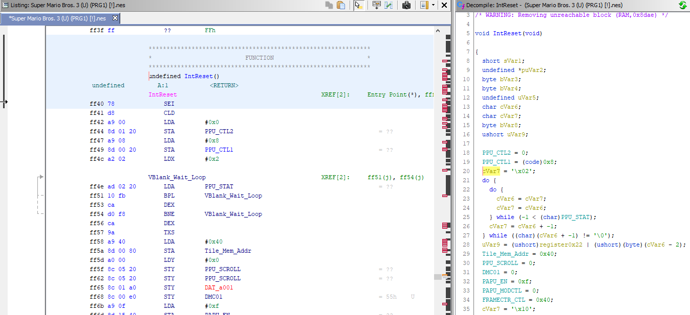 Super Mario Bros. 3 IntReset Disassembly and Decompilation via Ghidra